


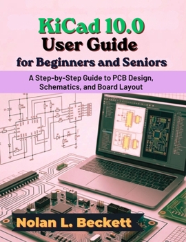
KiCad 10.0 User Guide for Beginners and Seniors

Have you ever wanted to design a printed circuit board but felt overwhelmed by schematics, footprints, routing, layers, libraries, and manufacturing files?
KiCad 10.0 User Guide for Beginners and Seniors provides a clear, practical, and step-by-step introduction to PCB design using one of the most powerful free electronic design automation platforms available.
Written for complete beginners, older learners, electronics students, hobbyists, makers, and aspiring engineers, this guide explains the complete KiCad workflow in simple language. You do not need previous PCB design experience or advanced engineering knowledge to get started.
Instead of relying on confusing tutorials or scattered technical information, you will follow a structured path from your first circuit idea to a finished board ready for production.
Inside this guide, you will learn how to:- Install and configure KiCad 10.0 correctly
- Navigate the Project Manager, Schematic Editor, and PCB Editor
- Understand electronic components and basic circuit diagrams
- Create clear and professional circuit schematics
- Work with symbols, footprints, component libraries, and 3D models
- Assign the correct footprints to physical components
- Create custom symbols and footprints
- Transfer a completed schematic into the PCB Editor
- Place components and define the board outline
- Route copper tracks and use vias effectively
- Set track widths, clearances, copper zones, and ground planes
- Run Electrical Rules Checks and Design Rules Checks
- Identify and correct common ERC and DRC errors
- Inspect completed boards with the KiCad 3D Viewer
- Generate Gerber files, drill files, bills of materials, and fabrication documents
- Prepare a PCB design for professional manufacturing
- Build LED, sensor, power supply, and microcontroller projects
- Troubleshoot missing libraries, incorrect footprints, routing issues, and manufacturing errors
Every important concept is explained gradually, with short sections, practical steps, common mistakes, and useful design tips. You will learn not only which tools to select, but also why each stage of the PCB design process matters.
This guide is ideal for:
- Complete KiCad beginners
- Seniors and older learners
- Electrical and electronics engineering students
- Arduino and Raspberry Pi users
- Robotics and embedded systems learners
- DIY electronics makers
- STEM students and educators
- Hardware developers and startup founders
- Hobbyists creating custom circuit boards
By the end of this book, you will understand the complete workflow:
Idea → Schematic → Components → Footprints → PCB Layout → Routing → Testing → Manufacturing
Stop feeling intimidated by PCB design. Develop practical skills, avoid expensive fabrication mistakes, and start creating cleaner, more reliable electronic projects.
Begin your KiCad journey today and turn your circuit ideas into real, professional-quality printed circuit boards.
Customer Reviews
ThriftBooks ® and the ThriftBooks ® logo are registered trademarks of Thrift Books Global, LLC