


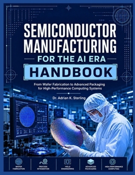
Semiconductor Manufacturing for the AI Era Handbook: From Wafer Fabrication to Advanced Packaging for High-Performance Computing Systems

From Wafer Fabrication to Advanced Packaging for High-Performance Computing Systems
What happens between semiconductor design and the finished AI chip?
Behind every AI accelerator is a highly coordinated manufacturing system involving materials, nanometer-scale patterns, contamination control, process variation, defects, yield, packaging, testing, and production efficiency.
Semiconductor Manufacturing for the AI Era Handbook takes you inside this system and explains how modern semiconductor manufacturing works as one connected engineering process, where every decision can affect performance, yield, reliability, cost, and capacity.
What You'll Discover Inside Semiconductor Materials & Wafer EngineeringSilicon crystal growth, wafer preparation, defects, resistivity, surface quality, contamination, engineered substrates, and wafer qualification.
Cleanrooms & Fab InfrastructureContamination control, ultrapure water, process gases, vacuum systems, environmental control, vibration, and facility reliability.
Thin-Film EngineeringOxidation, CVD, PVD, ALD, epitaxy, interfaces, film stress, conformality, uniformity, and process control.
Photolithography & Advanced PatterningPhotoresist, optical imaging, critical dimensions, overlay, EUV, multiple patterning, computational lithography, and process-window control.
Plasma Etching & Pattern TransferAnisotropic etching, selectivity, aspect-ratio effects, loading, profile control, endpoint detection, plasma damage, and 3D structures.
Metrology, Process Control & YieldLearn how manufacturers measure variation, detect defects and excursions, investigate failures, and improve manufacturing yield.
Memory, Chiplets, HBM & Advanced PackagingExplore silicon interposers, redistribution layers, TSVs, wafer thinning, hybrid bonding, microbumps, heterogeneous integration, chiplets, and high-bandwidth memory.
AI-Enabled Smart FabsDiscover how AI and machine learning support process monitoring, excursion detection, predictive maintenance, factory scheduling, and manufacturing optimization.
Manufacturing Economics & CapacityUnderstand yield, throughput, cycle time, bottlenecks, capital investment, packaging capacity, and cost per good die.
Built for Engineers and Technology ProfessionalsIdeal for engineering students, semiconductor professionals, manufacturing engineers, technical managers, researchers, and technology professionals who want to understand the bigger picture.
Rather than presenting disconnected process recipes, this handbook focuses on physical mechanisms, process interactions, engineering trade-offs, variability, measurement, yield, reliability, and manufacturability.
You'll find worked examples, quantitative reasoning, figures, tables, practice problems, key equations, and engineering case studies to strengthen practical understanding.
Why This Handbook MattersAI hardware is moving semiconductor manufacturing beyond transistor scaling. Greater performance now demands higher memory bandwidth, advanced interconnects, thermal management, sophisticated packaging, higher yield, and intelligent factories.
From crystal growth and wafer fabrication to lithography, etching, interconnects, HBM, chiplets, advanced packaging, and AI-assisted process control, this handbook gives you a clear framework for understanding the complete manufacturing chain.
Follow the wafer. Understand the process. Think like a semiconductor manufacturing engineer.
Customer Reviews
ThriftBooks ® and the ThriftBooks ® logo are registered trademarks of Thrift Books Global, LLC