Modeling MOSFET Gain Compression And Quasi-Sat Behavior: High Voltage MOSFET Model For Lightly Doped Drains

To model this non-linear behavior, a VBE multiplier (Q1, etc.) and Zener (D2), (see Figure 3) are used to mimic the non-linear behavior of the device near where ID shows a maximum. To model the quasi-sat behavior from the lightly doped drain variable resistance, a polynomial voltage controlled modeling circuit (E1) is used to mimic this non-linear aspect of the device.
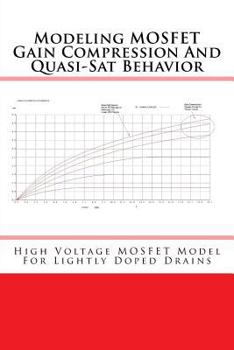
The gain compression and quai-sat behavior of lightly doped drain MOSFETs can be modeled by using the full gain compression circuit shown in Figure 3. This can be very valuable to accurately simulate the current-voltage behavior of lightly doped drains in high voltage/power MOSFETs. Both the gain compression (gm fall-off) and quasi-sat (variable effective drain resistance) behavior can be accurately modeled and simulated by the subcircuit model shown in Figure 3. By proper setting of the various circuit elements and their model parameters very accurate current-voltage behavior of lightly doped drain MOSFETs can be simulated to obtain accurate gate-source and gate-drain capacitances
Customer Reviews
ThriftBooks ® and the ThriftBooks ® logo are registered trademarks of Thrift Books Global, LLC